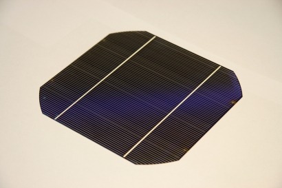
Currently, silicon solar cells convert an average of 14-19 percent of the incident solar energy into electricity, with more than 80 percent of them based on crystalline silicon. The goal of industry and research is to further optimise the cost of silicon solar cells, the “workhorse” of photovoltaics.
Fraunhofer researchers said the transfer of their research results into the production arena, concurrent with rapid market development in Germany, will help even further to reduce the costs of photovoltaic electricity.
“Just now, we were able to conclude several areas of development work on crystalline silicon solar cells. The results that we achieved belong to the best in the world,” said Christian Schmiga, project leader for high efficiency silicon solar cells at Fraunhofer ISE.
The investigated cell structures distinguish themselves in the type of silicon material, the so-called base, and in the type of emitter, a thin layer which collects the electrical charge carriers. Solar cells with a negatively conducting base are referred to as n-type and those with a positively conducting base as p-type cells. The emitter always has the inverse polarization of the base.
“For processing the emitter layer, we used three different procedures as follows: aluminium alloying and boron diffusion for the p-emitter layer of our n-type solar cells and phosphorous diffusion for the n-emitter layer of our p-type solar cells,” Schmiga said.
For an n-type silicon solar cell with aluminum-alloyed emitter, the researchers reached a record efficiency of 19.3 percent. To form the emitter, they screen-printed a paste containing aluminium, followed by a short high temperature firing step.
The team then conducted another test with a boron-diffused emitter whose surface was coated with an additional, new layer of aluminium-oxide.
On this test, Armin Richter, a Ph.D. student at Fraunhofer ISE, demonstrated an efficiency of 19.6 percent.
The researchers also achieved a 19.6 percent efficiency rate for p-type solar cells with phosphorous diffused emitter using the laser-fired contact (LFC) technology, developed and patented by Fraunhofer ISE.
All of the solar cells were processed on 125 x 125 mm² monocrystalline silicon wafers. A big advantage is that no additional adjusting or structuring steps were necessary, thus both simplifying and accelerating the processing procedure.
For additional information:

